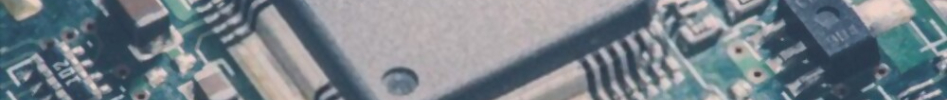
Key Considerations to Make When Assembling High-Density PCBs
There has been a rise in demand for faster and more capable electronics with the evolving technology. Currently, users opt for compact-sized, yet more powerful electronic devices with enhanced signal strength and improved reliability. To achieve this, PCBs, which are the backbone of all electronic products – are designed with advanced design approaches and manufacturing processes. Here comes the relevance of high-density PCB assembly that is characterized by higher wiring density per surface area than standard PCBs. HD design is slowly becoming the norm due to the demand for signal integrity and compact PCBs. It plays a significant role in improving electrical performance owing to its special assembly of thinner spaces, smaller vias, and a higher connection pad density. However, to achieve the desired performance, entire design process of high-density PCB assembly process must follow certain guidelines. This post aims to give you some basic insights on the best practices to be followed during high-density PCB assembly process.
Best Practices in High-Density PCB Assembly
There is a great demand for high density boards that are used in computers and smartphones, military communication systems, diagnostic and monitoring equipment, and missile and defense systems, among others. To meet the accurate demands of these mission-critical applications, HD boards are designed by following different fabrication and assembly processes than typical circuit boards. Following are a few of best practices that the PCB manufacturers follow during the design and assembly of high-density boards.
- Stack-Ups: The foundation of every HD board is the stack-up, which involve the proper arrangement of layers of copper and insulators. Working with the right stack-up not only increases routing density, and guarantees impedance-control but also contributes to high-speed signal transmission. High-density interconnect circuit boards require a carefully conceived stack-up to make the routing and layout tasks much simpler. HD stack-ups can range from several layers up to dozens in different configurations. A few points to note here include;
- For tight coupling, signal layers should be placed near the internal power layers
- From the top and bottom layers inward, create a symmetric stack-up
- Placing the most often utilized layers on top of the stack-up
- Micro-vias: Replacing the most common vias like blind, buried, or through-holes with micro-vias highly benefit HD design as it allows for greater routing densities on the board. Manufacturers also use a combination of regular thru-hole, blind and buried, and micro-vias to reduce the number of layers and material costs.
- Component Placement: Overcrowding of components is something that affects the integrity and signal strength of HD boards. In an urge to produce compact boards, PCB manufacturers tend to make the mistake of placing components nearby, leading to Electromagnetic Interference (EMI). Placing components leaving desired space also reduces stress, thereby adds to its signal strength.
- Component Selection: Through high-density PCB design, PCB manufacturers majorly aim to bring down costs and surface area. Hence, it is critical to choose a minimal number of components in HD boards. Moreover, it is mandatory to evaluate the Tg – Glass Transition Temperature, CTE – thermal coefficient of Z axis expansion, Td – Decomposition temperature, and other crucial properties of the materials selected as they determine the design of trace widths, locations, types and sizes for drill holes and stack up.
Following the aforementioned tips for HD PCB electronics manufacturing helps lowering costs, increase circuitry density, augment signal integrity and performance, and improve thermal management. As high-density PCBs represent one of the fastest-growing segments of the PCB market, manufacturers are constantly reinventing themselves to offer the best service. To successfully build high-density printed circuit boards, you need to partner with an expert manufacturer like Accelerated Assemblies who understands both the manufacturing requirements and the design. Being an experienced manufacturer and assembler of printed circuit boards, Accelerated Assemblies use advanced processing techniques, cutting-edge equipment, and expertise to produce HD boards. Talk to an expert at the firm and seek clarity on your questions and concerns about HD PCB manufacturing.