Boundary Scan Testing for PCB Assemblies and Its Benefits
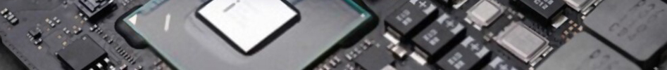
The electronic technologies have changed over the years. However, the printed circuit boards (PCBs) still form an integral part of electronic devices. Hence, it is also important that the PCBs perform to the highest standards. This is only possible when all components in the board function properly. Experienced PCB manufacturers take care to incorporate stringent testing at each phase of manufacturing to avoid its chances of failure in a real environment. These boards are subjected to different testing methods to check their overall quality and performance before being incorporated into any device. One of the popular testing methods is boundary scan testing. Unlike other testing methods, a boundary scan testing enables users to access and test individual traces on the circuit board, which is in function. This technique helps engineers to deeply focus on interconnects and ICs on the circuit boards and analyze their performance in real environments. For PCB manufacturers and service providers, this is one of the important steps in testing PCB assemblies and fabrication. This post discusses everything about boundary scan testing along with its benefits. So, stay tuned.
What is a Boundary Scan Testing?
The boundary scan testing is popularly known as JTAG testing because it follows the procedures described by the Joint Test Action Group (JTAG). A JTAG compliant IC has boundary scan cells or logic cells that are positioned between the signal balls or pins and the logic system of the chip. During the testing mode, these cells control both input and output pin status. This helps test the interconnections and boards easily.
How does a Boundary Scan Testing Work?
The logic cells can be operated in two modes - the test mode and the functional mode. Here is how the logic cells work in the test mode.
- The testing equipment is connected to the device and the signal is transmitted to the TDI input pin of the device.
- Through the input pin, it is transmitted to the logic cells, which further transmits it to the core logic.
- At the core logic, the signal is scanned. Then the TDO pin shifts the output through the core.
- A comparison is made between the output and the ideal result. These comparisons enable test engineers to identify faulty components and manufacturing defects, which are often not visible with the naked eyes in the case of denser circuits.
- The cells can be configured for external and internal testing modes. The chip logic is tested in the internal mode and the strength of interconnects between the board and the ICs in the external mode.
In the functional mode, the logic cells operate normally and they do not interfere with the device operation. However, in the test mode, the connection between the functional core and the pins are disconnected. The logic cells in this mode control the device value onto the net. This device is usually the JTAG enabled device. Today, most boards are equipped with JTAG headers for debugging or programming, which minimizes the need for test design.
Benefits of Boundary Scan Testing for PCB Assembly
The following beneficial features of the boundary scan testing have contributed to their popularity.
- The boundary scan reduces the test development costs because it uses a simple interface to control the IO pins that interact with devices under the test.
- These tests require no expensive fixtures and including boundary scan cells at the board level helps in the production as well as testing. In the production phase, it is used for programming. This programming, in turn, helps reduce the handling operations, as well as steps involved in the manufacturing.
- JTAG requires shorter testing times than other types of testing.
- JTAG testing assures a high level of fault information, which enables engineers to detect the defects earlier and make all necessary corrections. It helps engineers to identify the fault in a physical location, as well as on the schematics of the board.
Owing to all these reasons, boundary scan testing, which has been in use for several years now, is still popular with many PCB manufacturers. Many industry-leading names like Accelerated Assemblies, who offer PCB assembly services, utilizes boundary-scan testing to ensure error-free products.