A Focus on Assembly Manufacturing Technology and Processes Involved
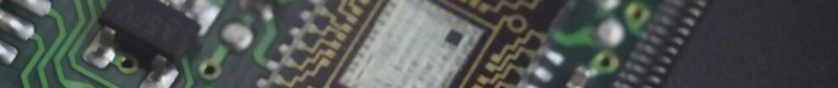
Almost all electronic devices used today function with printed circuit boards (PCBs) at their core. The compact yet crucial electronic board brings life to many devices. PCBs are manufactured as blank boards using several materials such as copper, aluminum, fiberglass, and so on. The assembling is done by mounting many small and fine components and making the circuit functional. Although PCB assembly seems easy, it has a lot of layers or steps. Also, with the increasingly complex device designs, features, and functionalities that are required, PCBs are also complex to be able to cater to these requirements. This complexity comprises compact sized boards, multiple components, a huge number of layers, and more. If there are any discrepancies or errors at any of these stages which are not rectified, it drastically impacts the performance of the final product, may lead to its non-functioning, or even cause shorting. Thus, it is of utmost importance to follow the PCB assembly steps to rightly assemble the blank boards. Would you like to know all this in detail? This post discusses PCB assembly manufacturing technology and processes at length.
Best Practices in PCB Assembly
PCBs have gained immense traction and are used in basic as well as advanced electronics applications, such as computers and smartphones, medical equipment, communication systems, satellite and navigation systems, and much more. To meet the demand of these challenging applications, PCBs must be designed using a reliable software as well after taking all the application requirements into consideration. Using the right technologies and processes for manufacturing as well as assembling PCBs is key. Following are a few best practices PCB manufacturers and assembly service providers follow during the design, manufacture, and assembly of printed circuit boards.
- After the design is final, the PCB making process comprises two main stages – the first is to manufacture the basic or bare circuit board, and the second is to populate it with small and big components vias, wires, heat sinks, copper traces, and more. PCB assembly demands two important files - the bill of materials (BOM) and the component placement list (CPL). Sometimes referred to as a product structure, BOM contains the part name, part number, product code, unit of measure, quantity, size, and required specifications or features of the product. Both CPL and BOM are a must right from the design stage and in fact once the list of materials and components is finalized. As the name implies, CPL defines the position of every component on the circuit board.
- The availability of the required components must be checked in advance with the vendors. The service provider must ensure they can be procured on time or just before assembling. If the specified components are unavailable or not in stock, then they will be sourced using an API system linked to the prominent component suppliers. Once is the components are ready, the next step is to apply the solder paste. This can be done using a stencil made of a thin metallic sheet. The solder paste stenciling ensures that the solder paste is applied to the area where components are mounted. The stencil is taken off the board after the application of solder paste.
- Next is pick and place component mounting, which can be performed either manually or mechanically through an automated system. In the case of through-hole PCB assembly, the component mounting is performed manually, while in surface-mount, it is performed by an automated machine. Compared to manual mounting, automatic component mounting is a precise, quick, and error-free process.
- All small and fine components are joined on the circuit board through soldering. Wave soldering is ideal for the through-hole assembly; wherein mounted components travel over a pan of molten solder. While in the surface-mount assembly, reflow soldering is used. Here, the solder paste of powdered solder and flux is used to attach components onto the board. One must ensure the components are firmly in place and other factors such as heat sinks for ventilation, solder joints and wires, and so on.
- Once done with the above process, it is important to conduct an inspection and quality check. This helps ensure the functioning of the device. Inspection can be done using three ways – visual inspection, automatic optical inspection (AOI), and X-ray inspection. Manual or visual inspection can only inspect the errors visible to the eyes. AOI machines have high-resolution cameras. They can be aligned in different angles for in-depth testing. Thus, this method is best suited for single- and double-sided PCBs. X-ray inspection is ideal for complex PCBs, which are hard to inspect.
- Once the inspection is performed, PCBs are tested for functionality, such as solderability test, contamination test, micro-sectioning test, and much more.
Following the above-mentioned tips for PCB assembly manufacturing helps lower the overall costs, increase circuit density, and achieve many other benefits. PCBs are being one of the fastest-growing segments of the electronic industry. Thus, manufacturers are strictly adhering to their assembly manufacturing technology and processes. To build high-quality and performance-driven circuit boards, you need to partner with a prominent manufacturer like Accelerated Assemblies, who thoroughly understands your requirements and the design. As an experienced PCB manufacturer and assembler, Accelerated Assemblies uses advanced processes, cutting-edge equipment, and skilled expertise to produce quality boards and assemblies.

